Hardware – Clock and Data Recovery
Clock and data recovery is an essential physical-layer function of modern switch and router hardware. Digging deep into the electronics of a router may not be your thing, but clock recovery is a fundamental building block for other network hardware functions. For example, serial to parallel data conversions require reliable clock and data recovery (CDR) to function effectively. It’s hard to understand serial to parallel conversions or signal conditioning without learning about CDR first.
Over-clocking to support 64b/66b
From the perspective of the transmitter’s MAC-layer, the bit rate of 10GBase-R is 10Gbps. (10Gbase-R here refers to SR, LRM, LR, ER etc.) On the physical line however, the bit-rate is 10.3125 Gbps. The 10Gbase-R link uses 64b/66b encoding which divides the Layer-2 data received from the MAC layer into 64-bit blocks and inserts an additional 2 bits of header before each block. This overhead does not eat into the available bandwidth. Instead the transmitter uses ‘over clocking’ and transmits the encoded bit-stream using a 10.3125 Khz clock. These additional bits are stripped by the receiving physical layer circuits and so the line-coding and over-clocking isn’t visible to the MAC layer. The rabbit hole on 64b/66b encoding goes a lot deeper, but for now it’s good to know that 64b/66b encoding exists.
In a 10GBase-R digital receiver, the received signal is interpreted by sampling the waveform right in the middle of the expected bit period. In order to align this sampling and properly decode the received signal as a one or zero, you need to have a receive clock which runs at precisely same frequency and phase as the transmitter’s clock. Unfortunately, you can’t just install the same 10.3125Khz oscillator in the receiver and be done with it. No….that would be too easy….
Clock and Data Recovery
The snag is there is that no oscillator is perfect. The 802.3 10G standard allows for the clock to be accurate to within +/- 0.01 percent. So it’s quite likely that the transmit and received clocks will be out-of-sync. This is called clock or frequency drift. Mismatched clocks will cause lost bits due to bit-slip or falsely interpreted bits where the receiver samples at the wrong point in the wave form, confusing a ‘one’ with a ‘zero’ or vice-versa.
The diagram below shows the Rx clock (in red) running faster than the Tx clock and data signal. Although the phase of the first 0-1 transitions are in-phase between the two signals, within a few clock cycles they’re in complete anti-phase. Yes, this is an exaggeration but it’s a real problem.

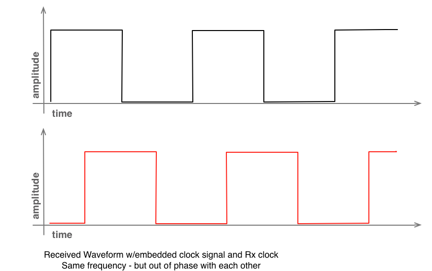
Even if the Tx and Rx clocks are running at precisely the same frequency, they would still need to be aligned so that their phases match each other. You can see a diagram below showing the clocks running at the same frequency but out of phase with each other, again leading to mis-sampling of the received signal.
Phase locked loop
“He’s got ….. lock on us! – He’s engaging me. Goddamn it. Mustang, this bogey’s all over me”
Instead of trying to guess the precise frequency and phase of the transmitter, why not derive it from the incoming signal? This is clock and data recovery (CDR). The CDR function built into a receiver has it’s own oscillator and uses a clever component called a phase locked loop (PLL) to calibrate the oscillator and match it to the phase and frequency of the incoming signal. Within the PLL there is a ‘phase comparator’ which compares the phase of the receive signal against the phase of the local oscillator. The difference between the two signals creates an output signal which drives the voltage controlled oscillator (VCO). This VCO control input modifies the oscillator to better match the incoming signal and feeds the local signal back into the phase comparator to start the process again.
I know, I’m losing you, but we’re done with the crazy electronics speak. The feedback circuit eventually locks the local oscillator onto phase and frequency of the incoming signal. That’s it. Once your PLL clock is ‘locked’ the receiver can correctly time it’s sampling to recovered the transmitted data. The transmitter’s clock can vary it’s frequency over time and temperatures though, so the PLL has to maintain that lock by continuously monitoring the received signal.
Transitions and line codes
I have hand-waved over an important element of clock and data recovery – level transitions. A level transition is a change from a one value to a zero value and from a zero to a one. In the examples above the bit stream was an idealistic square wave, 1-0-1-0-1-0. In the real-world, if there are no level transitions in a received data stream (e.g. a stream of all one’s or all zero’s) then the PLL loses it ability to detect the the clock speed of the transmitter. This is called ‘loss-of-lock’. The ‘run-length’ of a PLL is a measure of how long it can tolerate a lack of transitions before it loses lock.
The transmitted signal needs to be modified in some way to help the receiver recover and maintain their clock lock. 10Base-T Ethernet used Manchester Encoding which guaranteed a level transition during every bit time. Unfortunately it did this by doubling the clock frequency on the line, using two clock pulses for every data bit transmitted. That’s a 100% line-coding overhead.
In 10GBase-R the 64b/66b line coding addresses this problem. The two overhead bits (or preambles) can only have values 0-1 or 1-0. The 0-1 preamble means that the following 64-bit block is pure-data, and a 1-0 preamble means that the block contains some control information. We’ll explore the signaling later, but note that the 0-1 and 1-0 preamble patterns ‘guarantee’ a level transition every 64-bits. So we can say that 10GBase-R has a maximum of 64-bit ‘run-length’. The line-coding overhead is 3.125% which is more palatable than the manchester encoding overhead.
Furthermore, the 64-bit block is ‘scrambled’ to ensure further level transitions. This isn’t done solely for clock-recovery and makes it highly likely that you’ll have level transitions in your data stream, so it’s good to have the forced transitions from the 2-bit preambles.
Where is clock recovery used?
When the received serial 10GBase-R bit stream is to be transmitted to the MAC layer it has to be converted for transmission to the MAC using the XGMII interface 32-bit parallel interface. The Serial-in / Parallel-out (SIPO) converter needs to perform CDR here. The recovered data bits are clocked into a 32-bit register at line rate. The recovered clock is divided by 32 and used to clock the 32-bit words onto a bus at a reduced data rate.
Sometimes you want to perform CDR even when you plan to re-transmit the received serial data as another serial data stream. This is a form of re-conditioning and is known as re-timing. Signals transmitted in a channel will be attenuated (reduced in size) and distorted (changed in shape) as they travel, and as discussed in a prior post the circuit board is a hostile environment. By recovering the clock and data and then regenerating the pulses you can extend the life of a signal.
Lastly, you should note that the CDR mechanism usually has a hidden companion called an equalizer or EQ. The EQ is another part of signal conditioning, boosting the high-frequency components of a received signal, cleaning it up so that the CDR circuit can have a fighting chance of spotting the level transitions. We’ll look at EQ circuits soon.
If you have any questions, corrections or general feedback, please let me know in the comments.
18 thoughts on “Hardware – Clock and Data Recovery”
Now this is pure and lovely geek talk! 🙂
Hey Fred,
Thanks man. I used to think I wasn’t a geek, but I think the evidence is out there now!
/John H
Hi, your articles are very nice and easy to understand. Thanks so much. If possible could you possibly write something on ethernet architecture. Specifically going through the PCS lanes and explaining terms like PMD, XAUI, SERDES etc as well as the details on the 10Gb standard.
Hi Ned,
Sure thing, but it’ll take a little time. I’m trying to discuss these foundational topics first so that XAUI/XGMII and PCS/PMA/PMD are easier to explain later on. Thanks for your feedback, it’s much appreciated.
/John H.
I concur!!!
Great post, it’s really hard to find proper information out there, I have a relatively simple question, it seems that the SFP+ manufacturing process has progressed quite a bit, the vendors are offering SFP+ transceivers with CDR functionality now, my questions is: is it compatible with other types of SFP+s and the equipment using it, does it add additional value/benefit to the network ?
Thanks and regards,
Hi Sarmed,
Thanks for the comment. I haven’t used an SFP+ with built-in CDR, so I’m afraid I can’t provide a definitive answer. I guess it depends on which direction the CDR is applied, but either way it would generate a higher-quality signal in edge-cases.
One downside I can see at first glance is that your power draw per SFP+ will be higher due to the additional active components. For example on this site http://www.neophotonics.com/products/product_127.aspx, I see a 1.5W max for the CDR enable SFP+ and 1W max for the non-CDR variant. Personally I wouldn’t take on the power, cost and potential failure risks without a very strong reason. E.g. a switch/router vendor recommending it strongly.
Your article is extremely easy to understand even good reference to those non-geek beginners.
However, CDR location (in module or by host) is preferred to mention as CDR matters in SFP, SFP+ design, and the host-module interface requirement difference between XFI and SFI. The SFI interface requirement greatly drove PCB industry.
I thought CDR is a key consideration during the transition from GbE to 10G because CDR’s power consumption can’t be afforded in a reduced small space as SFP+ intent. As result the SFI interface requires more strict PCB channel characteristic to get better signal quality to deliver signal for CDR executing line-decoding at the host side.
I might be wrong or this is just a small part for the overall CDR(re-timer) story. But I saw how critical and important role of the re-timer location is to determine design quality in 25G/40G/100G. It’s useful and meaningful to my learning in Ethernet hardware.
Best regards
Hello John,
Awesome piece of work!!
I am not an electronics engineer. So, can you please tell me what role the clock plays in a transmitter/receiver? In other words, how does the transmitter/receiver use the clock in transmitting a signal?
Hi Namritha,
The clock is used by transmitter to decide the precise instant at which it changes the voltage level on the line. e.g. from 0 volts to 3.3volts for a binary 1 and vice versa. The receiver needs the same clock signal to know the precise moment to look at the incoming waveform (called ‘sampling’) to determine it’s value.
/John H
Great article, John, thank you for your time and passion for explaining complex things in a simpler way.
But I would like to specify a few moments if you don’t mind.
First of all, MAC layer uses XGMII format to represent Ethernet data to PHY layer (PCS+PMA). XGMII is about to 1 control bit for every 8 bits of data which eventually means 8b/9b encoding. MAC might pack XGMII data as 32 or 64 bits chunks – 32b/36b or 64b/72b.
PCS receives that data and able to understand where is the real data and where are control blocks, thanks for control bits. Then those chunks might be finally encoded with 64b/66b using one of 16 predefined templates.
Nowadays MAC, PCS and PMA are part of a single chip, so there are much fewer interblock buses, but still, to simplify the conception it is essential to explain the process as separate steps.
I’ve made a straight-through python script (without any bitwise actions and tricky translations) to visualize the process of encoding Ethernet data to XGMII format and then recording to 64b/66b – https://github.com/Sk1f3r/xgmii-64b66b
Once again, thank you for your articles and this one specifically.
Hey Sk1f3r,
Thanks for all the effort you put into this comment, I love your xgmii python work. This is why I wrote this post, to move the conversation forward and also to learn from my peers.
Thanks again,
John H
Hi,
Great article..
Can you please clarify your example diagrams with incoming data stream and sampled data at the receiver to make the problems more obvious. In the second example I thought local phased clock as generating the same data with simple phase shift but then I realized we are filling receiver data registers with the sampled data and introducing a bit shift in every octet and never fix it … Maybe it is more obvious for people smarter then me 🙂
Hi Ondy,
I don’t have cycles to edit the diagrams right now sorry. The intention of the examples is to show that that frequency mismatch and phase mismatch can both cause sampling errors. If unchecked you would indeed see continuous errors, but PLLs can and will correct this — assuming Rx signal is clean enough for the transitions to be detected.
Hi John.
I read many technical articles online and always thought that I understood the basics of that topics. After sometimes, I was not able to recollect.
But your article is very simple and able to understand the basics and very clear. I never forget this basics here onwards. Thanks a lot…
Delighted to have helped Devan, best of luck in your studies!
Amazing article on layer 1 technologies .