Hardware – How eye pattern diagrams work
Over the years I’ve seen the eye pattern diagram a few times. At first I don’t understand it and I get an instructor or peer to explain it. I briefly understand, then moments later… it’s gone. If you grok how this diagram is built straight away then please forgive me. Otherwise please read on.
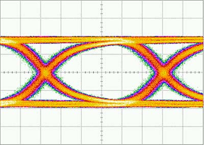
The eye pattern diagram is named after the eye shape in the middle of the diagram above. The purpose of the diagram is to measure the quality of the received electrical or optical signal. Put simply, the bigger the eye opening the better the signal. Before we dig deeper on the measurement we’ll examine how the eye diagram is made.
Constructing the eye diagram
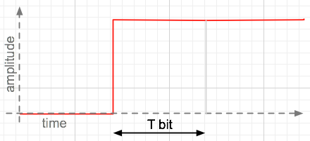
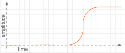
The ideal digital waveform is square and is all right-angles. The red diagram below shows three bit ideal periods (T) or Unit Intervals (UI). The digital values are 0, 1, 1.
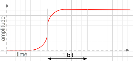
But real life digital signals don’t look like this. The waveforms get stretched, rounded and elongated. My waveform diagrams below aren’t totally accurate, but hopefully they’ll help you grok the concepts.
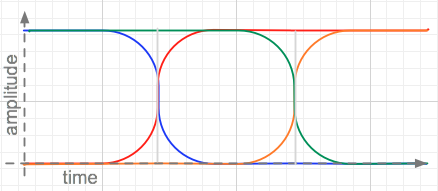
Let’s look at some other bit patterns. Here in green we have 1, 1, 0 pattern.

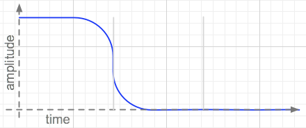
And the blue one here is a 1,0,0 pattern.
And finally a 0,0,1 in orange.
Putting it all together
The eye diagram is a pattern resulting from overlaying thousands of these permutations. The simplified view below shows what happened when you line up and overlay just four samples. Okay it’s not a complete match for the first diagram as it’s a bit too uniform, but we’re getting there.
So how is quality measured
Okay, so lets add a lot more samples of the waveform and see what happens when the world gets in the way. The height of the signal is reduced by attenuation, widening the horizontal lines. However when the bit transitions (1 to 0 and 0 to 1) are delayed things start to get a bit hairy, and it becomes harder to distinguish one transition from the other. The widening of these transitions is due to delay and is the manifestation of jitter.
The gray bars and diamond shape below are called the ‘signal compliance mask’. These mark out the limits of amplitude and time, and they mark the ‘keep-out’ areas for the signal. Interface standards like SFI, XFI, USB, SATA will specify signal standards using these signal compliance masks. If a single sample touches the mask, then the signal has failed the test.
 I
I
Sherpa Summary
I hope I’ve helped you understand eye-pattern diagrams a little better. You’ll often see these diagrams in Optical equipment marketing slides, but they apply just as well to electrical signals.
If you’re interested in learning more about signals, I found this OnSemi Eye-Pattern guide to be really useful and not overly technical. Please share any questions or clarifications in the comments.
8 thoughts on “Hardware – How eye pattern diagrams work”
Your two images do not match! In the second one compared to the first one, the signal rises too early, long before the clock suggested according to image one.
Hey Franky,
Yep, you’re dead right. It’s almost like the second graph is predicting the clock change. I’m not in a position to update the diagram right now, but will amend when time allows. Thanks for the comment and correction.
/John H
Is it possible to summarize the eyescan capability I see on certain HW. How is it done and plotted…
I’m afraid I’m not the engineer you’re looking for. Best to seek an electrical engineering blog to explore hardware capabilities for eye diagrams.