
We commonly interconnect network devices over distances of 100 meters for Cat5 Ethernet or maybe 300 meters over OM3 multimode fiber for 10GBASE-SR. With enough money we can extend the span between devices to perhaps 10Km for with 10GBASE-LR), 40Km for 10GBase-ER or even 80Km for 10GBase-ZR.
Why then, when we move to the world of circuit boards, do we have to suffer maximum distances which are measured in hundreds of millimeters? Let’s explore why life is so hard for the high-speed signals which transit the circuit board.

Why should you care?
Before we begin I’ve got to convince you why you should care. Okay, you’re definitely not going to see questions about circuits and traces on a certification exam. However, if you’re like me you’ll want to know a little bit more about how your routers and switches are put together. You may be painfully familiar with software bugs, but it’s important to note that vendors can design faulty hardware too. You should look at hardware designers as ‘humans solving extremely difficult problems’ – they can and do make mistakes.
For example, I saw an issue where the last two ports on the outer edge of a layer-3 switch encountered a problem with flapping interfaces. After much digging it turned out that the copper traces for those two SFP+ cages were longer that the traces of all the other ports. This additional length degraded the signal from those two transceivers to the point where the electronic dispersion compensation (EDC) chip couldn’t acquire the signal quickly enough, leading to a link bounce. In this case the problem could be fixed with a firmware update to the EDC micro-controller so all was not lost. The upside is that I’m now aware of a completely new class of problem that can exist due to circuit-board layout.
Circuit boards are hostile environments
A 10GBase-SR link has a maximum transmission distance of 300 meters on OM3 multimode fiber. The network engineer needs to maintain the integrity and cleanliness of that fiber so that a high-quality signal is transmitted between the transceivers at each end of the link. However the signal path doesn’t end at the transceiver. The electronic engineer designing the circuit board must ensure that the signal received by the transceiver is transmitted to the switch ASIC (and vice versa) whilst maintaining signal integrity – and that it a major challenge.
An SFP+ transceiver uses an electrical interface called SFI to communicate with the ASIC. The SFP+ transceiver has been optimised for size and power and thus has no signal conditioning hardware. The SFP+ transceiver will convert the 10GBase-SR optical signal into an electrical signal and transmit this directly to the ASIC without any doing clock-recovery or re-shaping.
So, having successfully travelled 300 meters across an optical fiber to the transceiver, the original 10GBase-SR signal can only travel 7 inches further along a modern circuit board before it becomes completely unintelligible. Luckily many modern ASICs, such as the Broadcom Trident+ are capable of receiving and interpreting the SFI-signaled 10Gbps signal directly. This approach is called a PHY-less switch and merits a complete post of it’s own. It is far more likely to have a chip, often called a PHY or SERDES, between the transceiver and the ASIC. These chips can perform some or all of the functions:
- Clock recovery and re-timing (common to all chips)
- Full electronic dispersion compensation – to deal with 10GBASE-LRM and 10GBASE-ER
- Electrical interface conversion (e.g. SFI to XFI, or SFI to KR)
- SERDES – Serial / Parallel conversion (e.g. single lane SFI to four-lane XAUI)
- PHY-layer sub-functions like the Physical Coding Sublayer (PCS).
I’ll give you the low-down on these chips in a later post, but all variants of these chips will regenerate and retime the received signal. This will buy you an additional 7 inches of reach between the SFP+ transceiver and the ASIC. If you need even longer reach you can implement 10GBASE-KR transceivers which can get you up to 1 meter across the backplane of a large chassis.
Circuit boards have always been hard to layout, but the number of buses and interfaces is increasing and the signal speed is going through the roof. Each of the signals traveling along the copper paths, or ‘traces’, has to deal with hazards like electromagnetic interference (EMI), coupling and crosstalk, signal reflections, impedance mismatches, skew, attenuation and a host of other threats as they travel. Your signal beautiful has left the coddled comfort of it’s noise-protected OM3 fiber, and arrived on the mean-streets of the circuit board which look an awful lot like a crowded radio spectrum. Let’s look at some of the circuit fundamentals and design choices.
Some fundamentals
The circuit board is constructed of copper paths, called ‘traces’ laid down on a board made of an insulating material called a ‘dielectric’. The most common and inexpensive dielectric material is called FR-4, then there is Nelco-4000. The most expensive dielectric, called Megatron-6, is many times the price of FR-4 but offers better signal protection which allows longer trace lengths.
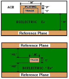
Why the jargon? I mention these dielectric and trace construction methods because the SFP+ specification (section 1.3) explicitly mentions these terms, and it’s good to have some background. Moreover the spec provides the maximum recommended lengths for each of these approaches.

Unfortunately there simply isn’t enough surface area on the circuit board to route all the required copper traces on it’s surface. Modern ASICS and CPUs come in a package called a Ball Grid Array (BGA), which have multiple rows of connectors around the chip. This means that you can’t use a single layer circuit board to fan-out all of these pins without risking the traces crossing over each other. Vendors address this by designing multi-layer circuit boards called a ‘stack-up’, which sandwiches multiple conductive layers and separates them with a suitable dielectric. The stack-up can have between two and twenty layers (or planes) to route circuits and often include a power-plane and one or more ground-planes.
Even with the stack-up of layers, some electrical paths will need to be routed between the layers, and this happens using special electro-plated holes drilled into the circuit. These are called ‘vias’ or through-holes. Of course there’s a catch here too. At high frequency these vias can behave like little antennae, adding further EMI and design complexity to the board. The need for differential signalling adds further complexity. Not alone does it double the number of traces, but the differential traces have to be sufficiently close to each other to ensure that noise impacts both the regular and inverted signal equally, i.e. tightly coupled. There is also the challenge of keeping trace lengths equal. Having irregular lengths on a multi-lane bus will cause a timing skew, where some bits in a word arrive earlier than others. Inconsistent trace lengths can also cause unexpected behaviour like the flapping-ports issue I described at the outset. Network engineering is hard, but I suspect that electrical engineering is harder.

Sherpa Summary
I know this was a long post, so thanks for reading this far. I hope you gained a little insight into the world of hard-core engineering problems hidden in modern circuit boards. As always, I’d love to hear your feedback; comments and corrections equally welcome!